|
|
Run Card for cmos150 |
|
Step 26.0 |
|||||||||||||||||||||||||||||||||
|
|
|
|
|
|||||||||||||||||||||||||||||||||
|
|
Process: Etch poly-Si in lam4 |
Date |
Operator |
|||||||||||||||||||||||||||||||||
|
|
|
|
|
|||||||||||||||||||||||||||||||||
|
1. |
Etch poly-Si in lam4. |
1/16/02 |
vorosl |
|||||||||||||||||||||||||||||||||
|
|
|
|
|
|||||||||||||||||||||||||||||||||
|
|
Average Etch time = 40 sec. Average Etch rate = 4300 A/min |
|
|
|||||||||||||||||||||||||||||||||
|
|
Recipe: 400 Power: 275 W |
|
|
|||||||||||||||||||||||||||||||||
|
|
Overetch : 225 W/ 20% |
|
|
|||||||||||||||||||||||||||||||||
|
|
|
|
|
|||||||||||||||||||||||||||||||||
|
2. |
Measure oxide thickness in S/D area of each work wafer. |
1/16/02 |
vorosl |
|||||||||||||||||||||||||||||||||
|
|
Nanospec, 10x |
|
|
|||||||||||||||||||||||||||||||||
|
|
|
|
|
|||||||||||||||||||||||||||||||||
|
|
|
|
|
|||||||||||||||||||||||||||||||||
|
|
|
|
|
|||||||||||||||||||||||||||||||||
|
|
|
|
|
|||||||||||||||||||||||||||||||||
|
3. |
Remove PR in O2 plasma (matrix). Piranha clean wafers in sink9 (MEMS). Dehydrate wafers in oven for > 30 min at 120C |
|
|
|||||||||||||||||||||||||||||||||
|
|
|
|
|
|||||||||||||||||||||||||||||||||
|
4. |
Measure channel length of the gate: Vickers and CDSEM |
|
|
|||||||||||||||||||||||||||||||||
|
|
Note: Vickers is not accurate for submicron features! CD measurement data from #1 wafer. |
|
|
|||||||||||||||||||||||||||||||||
|
|
|
|
|
|||||||||||||||||||||||||||||||||
|
|
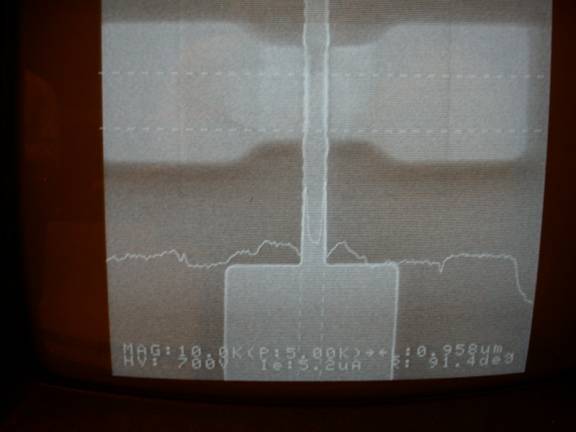
Measured gate length= 0.95 micron from device. |
|
|
|||||||||||||||||||||||||||||||||
|
|
|
|
|
|||||||||||||||||||||||||||||||||
|
|
Note: reworked
#3,#4,#10,#15!: All of them baked for 2 hours (at 120C), UVBAKE was down! Recipe, condition is the same and verified. First etched #3. Possible under baked. Tried to correct, finally over etched the poly.!!! #10 etch time: 60+7 sec #4,#15 etch time: 67+7 sec. Reason for extra etching time: oxide thickness on S/D area was too thick (350-400 A) measured by nanospec. Finally oxide thickness on S/D area [A]: wafer 1. point 2.point #15 186 184 #4 180 178 #10 199 201 Note: PR (UV210-0.6) thickness 4200A and poly thickness=4500A are very close. It seemed the selectivity almost ~1:1 PR: poly-Si. Remaining poly thickness: #10 4000 A #4,15 2000 A #3 zero!!! Measured with as200 on the pattern below the alignment structures. |
02/11/02 |
vorosl |